
Oct 12, 2026
5 Key Takeaways From electronica India 2026
5 Key Takeaways From electronica India 2026 Thousands of visitors. Hundreds of exhibitors. One li...
Smith’s team of experts brings a diverse wealth of knowledge and experience that helps us offer the most relevant and actionable insights into the global electronic-component marketplace. Follow Smith’s Market Blog to stay up to date on the latest information.
On Tuesday, July 28, at 4:27 PM JST (2:27 AM CDT), a 7.0-magnitude earthquake struck the Kumamoto prefecture of Kyushu, Japan’s “Silicon Island.” This is the highest level on the Japanese earthquake scale and only the eighth time a quake of this intensity has been recorded in Japan. Dozens of fatalities have been reported, while several dozen people remain unaccounted for.
The Japan Meteorological Agency has warned that significant aftershocks may continue for up to a week, though the first two to three days posed the highest risk. Some aftershocks could reach magnitudes approaching 7.0, and several events of approximately magnitude 5.0 or greater have already been recorded.
Kyushu’s “Silicon Island” nickname stems from the concentration of semiconductor- manufacturing facilities that have been established through decades of investment by leading chipmakers. Many of these facilities are located close enough to the affected area to face potential damage. Enhanced seismic building standards are offsetting some of this risk, which were implemented following the major Kumamoto earthquake in 2016 and improved the earthquake resilience of newer facilities and infrastructure.
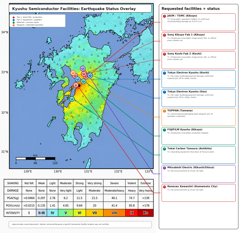
Facilities within the affected area experienced power interruptions and have suspended operations while damage assessments and safety inspections are conducted. Comprehensive inspections, including verification of critical systems and utilities, typically require one to two days to complete. Although some preliminary information has been released, more reliable assessments of facility conditions and restart timelines may not become available until later this week or early next week.
The impacted region represents multiple tiers of the semiconductor supply chain, including wafer fabrication, semiconductor equipment, materials, packaging, and component manufacturing. Recovery times vary considerably based on the operations, and any production interruptions could have differing implications for global supply chains.
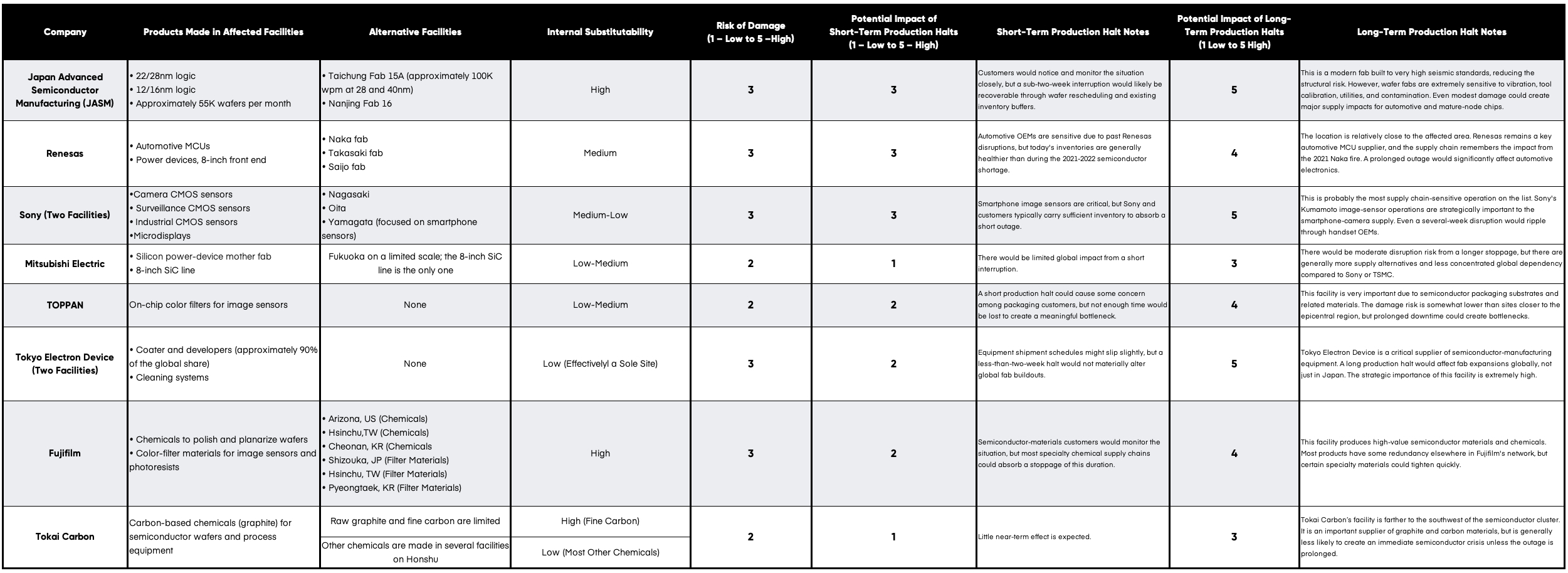
Among the facilities in the affected area, Renesas appears to present the greatest potential supply chain risk. Its site is among the closest major semiconductor facilities to the earthquake’s epicenter and produces automotive and industrial microcontrollers, including wafer-processing and -packaging operations that can be particularly sensitive to seismic events and power disruptions.
The company shared the following update on July 30:
“At the Nishiki factory, following confirmation of the safety of the cleanroom environment, production resumed in phases beginning on the evening of July 29.
At the Kawashiri factory, initial safety inspections within the cleanroom have been completed, and evaluations of the impact on equipment and work-in-process are ongoing. Preparations for the resumption of production are underway, and production is expected to resume in phases beginning on August 5.”
Its Nishiki facility resumed production in phases beginning on the evening of July 29, following confirmation of the cleanroom environment. At the Kawashiri factory, initial safety inspections within the cleanroom have been completed, and evaluations of the impact on equipment and works-in-process are ongoing. Preparations for the resumption of production are underway, and production is expected to resume in phases beginning on August 5.
Tokyo Electron Device Kyushu is also an important facility to monitor. As one of the world’s leading semiconductor-equipment suppliers, Tokyo Electron Device supports chip production globally through its deposition, etch, cleaning, and other wafer-fabrication tools. Any prolonged disruption could affect equipment deliveries, service support, and fab-expansion projects across the semiconductor industry.
Japan Advanced Semiconductor Manufacturing (JASM), a TSMC subsidiary, has restarted production at its foundry site while inspections continue to assess damages, though none have been reported yet. The site should return to its previous utilization rate within a week.
Ultimately, while many semiconductor facilities often require several weeks to fully restore production rates following an unplanned shutdown, the near-term market impact is likely to remain limited if inspections reveal minimal damage and operations resume within a relatively short timeframe.
We will continue to monitor the situation and share the latest updates as they become available.
5 Key Takeaways From electronica India 2026
5 Key Takeaways From electronica India 2026 Thousands of visitors. Hundreds of exhibitors. One li...
Smith Will Exhibit at electronica Munich 2026, Hall B5, Stand 341
The company will showcase its comprehensive suite of supply chain solutions and diverse service o...
Smith Will Exhibit at the 2026 New York Solar + Storage Summit, Booth 20
The company will highlight how it supports the solar industry with diverse supply chain solutions...
您可通过以下三种方式,轻松关注Smith微信公众号: